


A new architecture takes very few processing steps to produce an affordable solar cell with efficiencies comparable to conventional silicon solar cells. This new architecture uses alternative, transparent materials that can be deposited at room temperature, eliminating the need for high temperature chemical doping — the process currently used to increase the electrical conductivity of key surfaces in solar cells.
Proving that this simple design can lead to high conversion efficiencies, turning sunlight into electricity, makes it a useful tool to lower costs and improve performance of a wide range of solar cell designs. Additionally, this simple process could be extended to improve contacts in semiconductor transistors used to speed today’s computers.
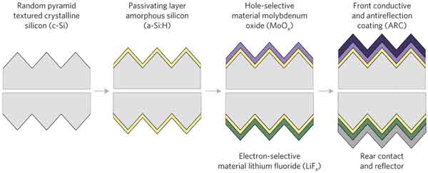
The cross-section shows key features of a new solar cell architecture. Textured silicon is coated and the required solar cell contacts are deposited at room temperature. A metal oxide layer is deposited on the sun-facing top and a metal fluoride layer is deposited onto the bottom. Additional coatings are added to managing light reflection. The new design produces a solar cell that rivals the performance achieved from cells made using conventional processing that requires heat and an ultra-clean environment. Image courtesy of Ali Javey of University of California, Berkeley
In this simplified architecture, sunlight passes through the top layer (metal oxide) and creates electron-hole pairs in the silicon. The holes are drawn to the molybdenum oxide layer, while the electrons are drawn to the lithium fluoride layer, which can be used to produce electricity.
This design uses a seven-step process and low-temperature processing to produce a device that efficiently separates photo-generated elections and holes. In this process, the crystalline silicon with a pyramid texture is coated with a passivating layer of amorphous silicon. Then, molybdenum oxide is deposited at room temperature on the top side of the device.
Molybdenum oxide advantageously is transparent, allowing the sunlight to reach the silicon core, and has the appropriate electronic properties to conduct the photo-generated holes. Next, lithium fluoride is deposited at room temperature onto the bottom side of the solar cell to draw the photo-generated electrons from the silicon core.
This simple, processing is less expensive than conventional processing for silicon solar cells that requires chemical doping at high temperatures to create contacts that separate the photo-generated electrons and holes. Impressively, the simplified architecture achieves solar energy conversion comparable to conventional silicon solar cells at a lower cost.
Reference(s):
Publication: James Bullock, Mark Hettick, Jonas Geissbühler, Alison J. Ong, Thomas Allen, Carolin M. Sutter-Fella, Teresa Chen, Hiroki Ota, Ethan W. Schaler, Stefaan De Wolf, Christophe Ballif, Andrés Cuevas, Ali Javey. Efficient silicon solar cells with dopant-free asymmetric heterocontacts. Nature Energy, 2016
Story: Department of Energy, Office of Science | June 24, 2016


Comments