


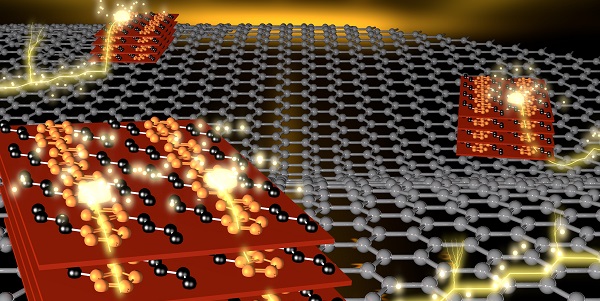
Graphene – a one-atom-thick sheet of carbon with highly desirable electrical properties, flexibility and strength – shows great promise for future electronics, advanced solar cells, protective coatings and other uses, and combining it with other materials could extend its range even further.
Experiments at the Department of Energy’s SLAC National Accelerator Laboratory looked at the properties of materials that combine graphene with a common type of semiconducting polymer.
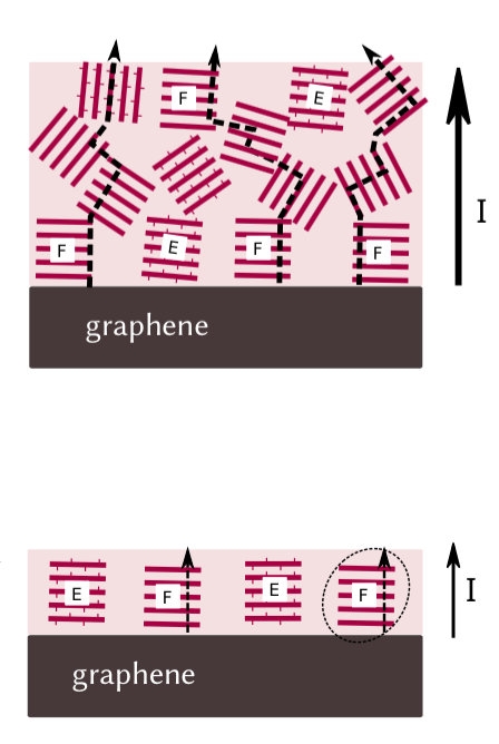 Studies conducted at the Stanford Synchrotron Radiation Lightsource revealed that when deposited atop graphene, a thicker polymer film (top) conducted charge significantly better than a thinner polymer film (bottom). This is likely because the orientation of the polymer crystallites within the thick film allows the formation of a continuous pathway for the charge to flow. Credit: David Barbero
They found that a thin film of the polymer transported electric charge even better when grown on a single layer of graphene than it does when placed on a thin layer of silicon.
“Our results are among the first to measure the charge transport in these materials in the vertical direction – the direction that charge travels in organic photovoltaic devices like solar cells or in light-emitting diodes,” said David Barbero of Umeå University in Sweden, leader of the international research team that performed the experiments at SLAC’s Stanford Synchrotron Radiation Lightsource (SSRL), a DOE Office of Science User Facility. “The result was somewhat expected, because graphene and silicon have different crystalline structures and electrical properties.”
But the team also discovered something very unexpected, he said.
Although it was widely believed that a thinner polymer film should enable electrons to travel faster and more efficiently than a thicker film, Barbero and his team discovered that a polymer film about 50 nanometers thick conducted charge about 50 times better when deposited on graphene than the same film about 10 nanometers thick.
The team concluded that the thicker film’s structure, which consists of a mosaic of crystallites oriented at different angles, likely forms a continuous pathway of interconnected crystals. This, they theorize, allows for easier charge transport than in a regular thin film, whose thin, plate-like crystal structures are oriented parallel to the graphene layer.
By better controlling the thickness and crystalline structure of the semiconducting film, it may be possible to design even more efficient graphene-based organic electronic devices.
“The fields most likely to benefit from this work are probably next-generation photovoltaic devices and flexible electronic devices,” said Barbero. “Because graphene is thin, lightweight and flexible, there are a number of potential applications.”
References:
Publication: Vasyl Skrypnychuk, Nicolas Boulanger, Victor Yu, Michael Hilke, Stefan C. B. Mannsfeld, Michael F. Toney, David R. Barbero. Enhanced Vertical Charge Transport in a Semiconducting P3HT Thin Film on Single Layer Graphene. Advanced Functional Materials, 2015
Story: Semiconductor Works Better when Hitched to Graphene | SLAC National Accelerator Laboratory — February 18, 2015


Comments