


New research breakthrough results may lead to eventual improvement in the conversion efficiency of CdTe solar cells.
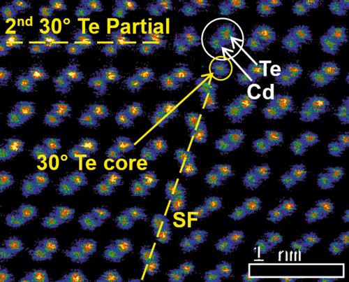
By using atomic-resolution Z-contrast imaging and X-ray spectroscopy in a scanning transmission electron microscopes scientists have successfully been able to explore dislocations in the binary II-VI semiconductor CdTe, commercially used in thin-film photovoltaics. These novel insights into atomically resolved chemical structure of dislocations have potential for understanding many more defect-based phenomena.
In-Depth Article:
Crystallographic defects or irregularities (known as dislocations) are often found within crystalline materials. Two main types of dislocation exist: edge and screw type. However, dislocations found in real materials tend to be a mix of these two types, resulting in a complex atomic arrangement not found in bulk crystals.
The study of these dislocations in semiconductors is probably as old as the science of semiconductors itself, and the technological importance of dislocations can hardly be overstated.
From their roles in the way crystals form to their effects on a material’s mechanical, thermal and opto-electronic properties, dislocation and defects govern many aspects of a material’s behaviour. Therefore, it is of great scientific interest to identify and study these structures, and understand their impact on the properties of technologically important materials and devices, such as solar cells, photon detectors and similar semiconductor devices.
Despite the large amount of theoretical work in this field, experimental knowledge detailing the atomically resolved chemical structure of even the most basic dislocations has just begun to be accessible.
A group of scientists from the United States has combined state-of-the-art atomic-resolution Z-contrast imaging and X-ray spectroscopy in a scanning transmission electron microscope (STEM) to analyse two low-elastic-energy stair-rod dislocations in the binary II-VI semiconductor CdTe. CdTe is commercially used in thin-film photovoltaics owing to its ideal electrical properties.
The conversion efficiency of CdTe solar cells, which is critical for the industry, has only seen minor developments and improvements over the last 20 years despite intense research activity. Current laboratory records are still shy of the theoretical limits quoted as far back as 1961.
In the current issue of Acta Crystallographica Section A: Foundations and Advances, Klie and co-workers demonstrate how, with the use of atomic-resolution STEM images and specially tailored Burgers circuits, the structure of these dislocations can be identified. The results may lead to the eventual improvement in the conversion efficiency of CdTe solar cells. The analysis presented by the authors can also be applied to study and predict similar structures in other zinc-blende and diamond materials.
This study further demonstrates how the new generation of aberration-corrected electron microscopes can advance our understanding of seemingly basic crystal-structure defects.
Publication Reference:
Tadas Paulauskas et al: Atomic scale study of polar Lomer–Cottrell and Hirth lock dislocation cores in CdTe. Acta Crystallographica Section A Foundations and Advances, 2014.


Comments