


A new collaborative research by scientists at DOE’s Lawrence Berkeley National Laboratory have uncovered the first experimental observation of ultrafast charge transfer in photo-excited MX2 materials.
What does this mean? For graphene, well–its no longer the next big thing for high technology. For Solar energy technology, this comes as great news as the charge transfer time of these materials were clocked in at under 50 femtoseconds, comparable to the fastest times recorded for organic photovoltaics.
In-Depth Article:
An international collaboration of researchers led by a scientist with the U.S. Department of Energy (DOE)’s Lawrence Berkeley National Laboratory (Berkeley Lab) has reported the first experimental observation of ultrafast charge transfer in photo-excited MX2 materials. The recorded charge transfer time clocked in at under 50 femtoseconds, comparable to the fastest times recorded for organic photovoltaics.
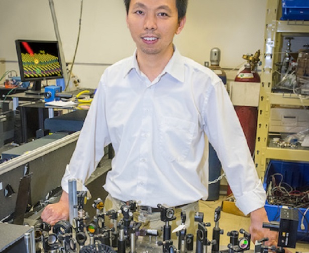
“We’ve demonstrated, for the first time, efficient charge transfer in MX2 heterostructures through combined photoluminescence mapping and transient absorption measurements,” says Feng Wang, a condensed matter physicist with Berkeley Lab’s Materials Sciences Division and the University of California (UC) Berkeley’s Physics Department. “Having quantitatively determined charge transfer time to be less than 50 femtoseconds, our study suggests that MX2 heterostructures, with their remarkable electrical and optical properties and the rapid development of large-area synthesis, hold great promise for future photonic and optoelectronic applications.”
Wang is the corresponding author of a paper in Nature Nanotechnology describing this research. The paper is titled “Ultrafast charge transfer in atomically thin MoS2/WS2 heterostructures.” Co-authors are Xiaoping Hong, Jonghwan Kim, Su-Fei Shi, Yu Zhang, Chenhao Jin, Yinghui Sun, Sefaattin Tongay, Junqiao Wu and Yanfeng Zhang.
MX2 monolayers consist of a single layer of transition metal atoms, such as molybdenum (Mo) or tungsten (W), sandwiched between two layers of chalcogen atoms, such as sulfur (S). The resulting heterostructure is bound by the relatively weak intermolecular attraction known as the van der Waals force. These 2D semiconductors feature the same hexagonal “honeycombed” structure as graphene and superfast electrical conductance, but, unlike graphene, they have natural energy band-gaps. This facilitates their application in transistors and other electronic devices because, unlike graphene, their electrical conductance can be switched off.
“Combining different MX2 layers together allows one to control their physical properties,” says Wang, who is also an investigator with the Kavli Energy NanoSciences Institute (Kavli-ENSI). “For example, the combination of MoS2 and WS2 forms a type-II semiconductor that enables fast charge separation. The separation of photoexcited electrons and holes is essential for driving an electrical current in a photodetector or solar cell.”
In demonstrating the ultrafast charge separation capabilities of atomically thin samples of MoS2/WS2 heterostructures, Wang and his collaborators have opened up potentially rich new avenues, not only for photonics and optoelectronics, but also for photovoltaics.
“MX2 semiconductors have extremely strong optical absorption properties and compared with organic photovoltaic materials, have a crystalline structure and better electrical transport properties,” Wang says. “Factor in a femtosecond charge transfer rate and MX2 semiconductors provide an ideal way to spatially separate electrons and holes for electrical collection and utilization.”
Wang and his colleagues are studying the microscopic origins of charge transfer in MX2 heterostructures and the variation in charge transfer rates between different MX2 materials.
“We’re also interested in controlling the charge transfer process with external electrical fields as a means of utilizing MX2 heterostructures in photovoltaic devices,” Wang says.
Publication Reference:
Xiaoping Hong et al: Ultrafast charge transfer in atomically thin MoS2/WS2 heterostructures. Nature Nanotechnology, 2014.


Comments